Burn-in Testing
/ /Burn-in Testing
Burn-in testing is the process by which a system detects early failures in semiconductor components (infant mortality), thereby increasing a semiconductor component reliability. Normally burn-in tests are performed on electronic devices such as laser diodes with an Automatic Test Equipment laser diode burn-in system that runs the component for an extended period of time to detect problems.

A burn-in system will use cutting-edge technology to test the component and provide precision temperature control, power and optical (if required) measurements to ensure the precision and reliability required for manufacturing, engineering evaluation, and R&D applications.
Burn-in testing may be conducted to ensure that a device or system functions properly before it leaves the manufacturing plant or to confirm new semiconductors from the R&D lab are meeting designed operating requirements.
It is best to burn-in at the component level when the cost of testing and replacing parts is lowest. Burn-in of a board or an assembly is difficult because different components have different limits.
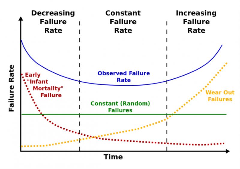
It is important to note that burn-in test is usually used to filter out devices that fail during the “infant mortality stage” (beginning of bathtub curve) and does not take into count the “lifetime” or wearout (end of the bath tub curve) – this is where reliability testing comes into play.
Wearout is the natural end-of-life of a component or system related to continuous use as a result of materials interaction with the environment. This regime of failure is of particular concern in denoting the lifetime of the product. It is possible to describe wearout mathematically allowing the concept of reliability and, hence, lifetime prediction.
What Causes Components to Fail During Burn-in?
The root cause of fails detected during burn-in testing can be identified as dielectric failures, conductor failures, metallization failures, electromigration, etc. These faults are dormant and randomly manifest into device failures during device life-cycle. With burn-in testing, an Automatic Test Equipment (ATE) will stress the device, accelerating these dormant faults to manifest as failures and screen out failures during the infant mortality stage.
Burn-in testing detects faults that are generally due to imperfections in manufacturing and packaging processes, which are becoming more common with the increasing circuit complexity and aggressive technology scaling.
Burn-in Testing Parameters
A burn-in test specification varies depending on the device and testing standard (military or telecom standards). It usually requires the electrical and thermal testing of a product, using an expected operating electrical cycle (extreme of operating condition), typically over a time period of 48-168 hours. The thermal temperature of the burn-in test chamber can range from 25°C to 140°C .
Burn-in is applied to products as they are made, to detect early failures caused by faults in manufacturing practice.
Burn In Fundamentally performs the following:
Stress + Extreme Conditions + Prolong Time = Acceleration of “Normal/Useful life”
Types of Burn-in Tests
Dynamic Burn-in : the device is exposed to high voltage and temperature extremes while being subjected to various input stimuli .
A burn-in system applies various electrical stimuli to each device while the device is exposed to extreme temperature and voltage. The advantage of dynamic burn-in is its ability to stress more internal circuits, causing additional failure mechanisms to occur. However, dynamic burn-in is limited because it cannot completely simulate what the device would experience during actual use, so all the circuit nodes may not get stressed.
Static Burn-in : Device under test (DUT) is stressed at elevated constant temperature for an extended period of time.
A burn-in system applies extreme voltage or currents and temperatures to each device without operating or exercising the device. The advantages of static burn-in are its low cost and simplicity.
How is a Burn-In Test Performed?
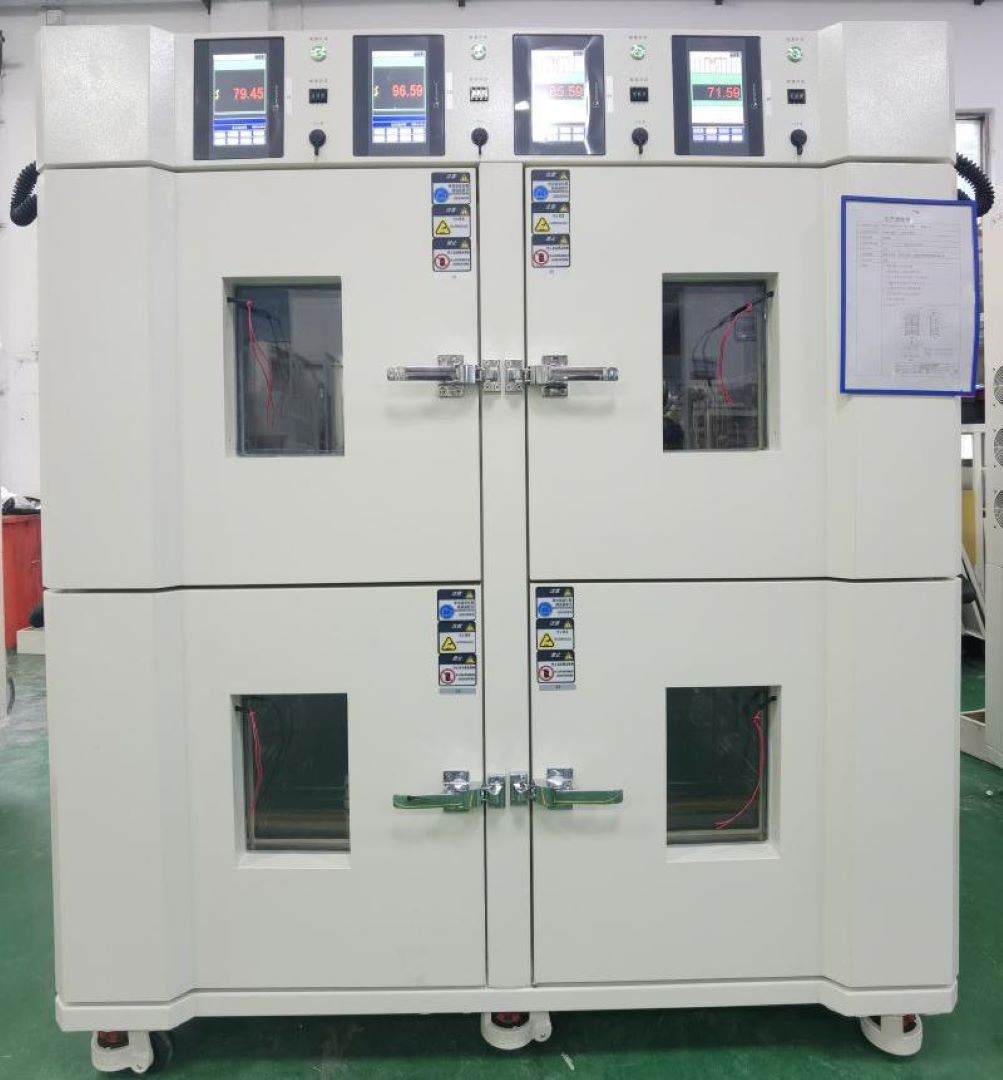
The semiconductor device is placed onto special Burn-in Boards (BiB) while the test is executed inside special Burn-in Chamber (BIC).
Know more about Burn-in Chamber(Click here)
